Patentix Inc.
- CEO
- Toyosuke Ibi
- Founded
- 2022
- Location
- Kusatsu-shi, Shiga

COMPANY OVERVIEW
Our core technological seeds consist of heteroepitaxial growth and bulk crystal growth techniques for rutile germanium dioxide (r-GeO₂), a novel power semiconductor material. As our primary solution, we provide r-GeO₂ semiconductor substrates to power device manufacturers. This enables the realization of next-generation r-GeO₂ power devices, ultimately driving substantial energy savings and achieving Green Transformation (GX) goals. By providing these advanced, ultra-wide bandgap substrates, we empower device manufacturers to create highly efficient components that minimize power conversion losses. Our proprietary technology serves as an essential foundation for accelerating decarbonization and advancing sustainable energy solutions across global power electronics markets.
SOLUTION
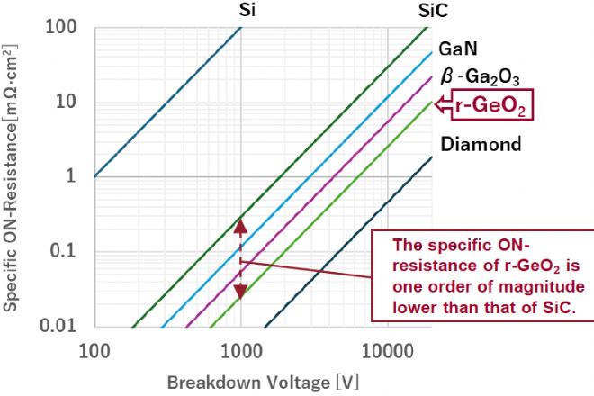
Power loss occurring during power conversion using power devices accounts for as much as 10% of total generated electricity. Widespread adoption of power devices using r-GeO₂ significantly reduces these conversion losses. By vastly improving energy efficiency across grid, industrial, automotive and data-center, applications, this groundbreaking ultra-wide bandgap technology directly minimizes overall energy consumption. Consequently, it lowers greenhouse gas emissions and fosters the highly efficient utilization of energy worldwide. Our r-GeO₂ solutions serve as a vital driver for achieving Green Transformation (GX), paving the way toward a carbon-neutral society through advanced, high-efficiency power semiconductor innovations and sustainable technology.
ORIGINALITY
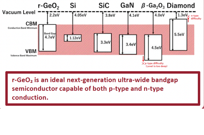
Rutile germanium dioxide (r-GeO₂) is the newest ultra-wide bandgap (UWBG) semiconductor, competing with Ga₂O₃, diamond, and AlN, as well as established WBG technologies like SiC and GaN. Globally, we are the only business entity publicly conducting r-GeO₂ R&D. While universities worldwide pursue basic research, we stand out as the sole organization developing heteroepitaxial growth on cost-competitive silicon substrates. This proprietary “GeO₂ on Si” technology overcomes conventional cost barriers, securing our unique position as the global leader capable of driving the rapid commercialization and market adoption of high-efficiency r-GeO₂ power devices for next-generation power electronics applications.
VISION
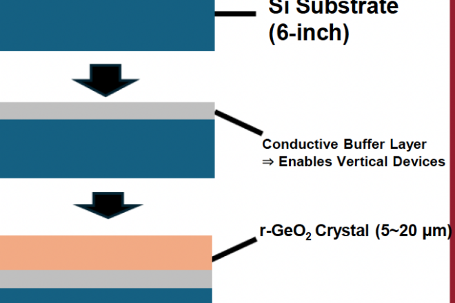
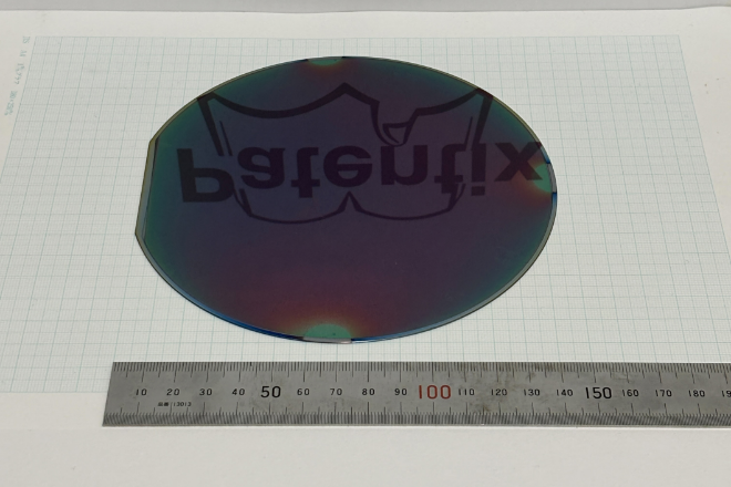
We have achieved “GeO₂ on Si” by heteroepitaxially growing r-GeO₂ thin films on 6-inch silicon substrates. We plan to ship samples to domestic power device manufacturers in Japan as early as 2026. “GeO₂ on Si” serves as a critical key technology designed to accelerate the social implementation of this novel semiconductor material. To bring this innovation to market, we have established a strategic roadmap aiming for full mass production of r-GeO₂ power devices by 2030. This achievement will establish a scalable foundation for next-generation, high-efficiency power electronics, significantly reducing energy losses across grid, industrial, automotive and data-center applications worldwide.
CONTACT US
For further information on the company, please contact from the link below